
![]()

About the Facilities
Lab: Cleanroom
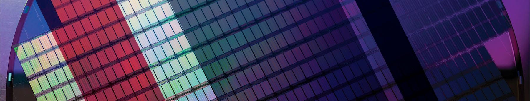
OPTOELECTRONIC PROCESSING FACILITY
This multi-user cleanroom is outfitted with advanced equipment for fabricating semiconductor and optoelectronic devices on a wafer-to-die level. The 2,500-square-foot facility includes both a Class 100 photolithography room and a Class 1000 cleanroom. In the Class 1000 cleanroom, capabilities include wet chemical processing, dry etching, thin film physical vapor deposition (including thermal oxidation and annealing), metrology, dicing saw, and wire bonding.
Lab: Characterization
PRECISION MEASUREMENT LABORATORY
This lab is a shared-use, core facility dedicated to the characterization of materials using scanning and surface probe microscopies. It also provides capabilities for examination of topographical features using optical laser interferometry profiling.
Lab: Microscopy
FOCUS ION BEAM/TRANSMISSION MICROSCOPY FACILITY
This multi-user facility provides equipment for materials characterization and high-resolution imaging and analysis of a variety of solid, non-biological materials on nanoscale. The facility is supplemented by an adjacent materials preparation laboratory with equipment for cutting, polishing, dimpling, and ion milling for preparation of surfaces and cross-sections from bulk specimens for examination. These capabilities will be key as semiconductor devices shrink into the nanometer range and new materials are required.
Lab: Materials Science
MATERIALS SCIENCE CORE FACILITY
This multi-user facility for materials science characterization houses a variety of equipment including processing hoods for materials preparation and Bruker X-ray equipment for analyzing crystallinity of thin solid-state films.