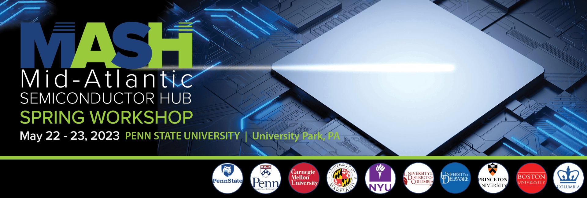
May 22-23, 2023
Penn State University
University Park, PA
This two-day workshop brings together semiconductor industries and institutions nationwide to discuss R&D opportunities under the CHIPS and Science Act. In January at University of Pennsylvania, the first MASH workshop focused on the needs of the industrial semiconductor sector. This workshop will focus on identifying industry-academia-government partnerships that will position the U.S. for technology and workforce leadership in semiconductors and microelectronics.
Workshop Featured Topics:
- Education and workforce development
- Silicon-adjacent materials
- Advancement of testing, assembling, and packaging capabilities
In addition to presentations by invited speakers from diverse organizations, there will be opportunities to work in focused groups to promote insightful analysis of the multiple challenges impacting the U.S. semiconductor industry.
Day 1:
| Monday, May 22* | ||
|---|---|---|
| REGISTRATION: Business Building Atrium | ||
| LOCATION: Agricultural Science and Industries Building (Room 101) | ||
| TIME | TOPIC | SPEAKER |
| 8:00-9:00 | Breakfast, Registration, Networking | |
| 9:00 | Welcome and Summary | Daniel Lopez Liang Professor of EECS, Director of the Nanofabrication Lab, The Pennsylvania State University |
| 9:00-9:20 | MASH: Setting a Course for America's Semiconductor Future | Neeli Bendapudi President of the Pennsylvania State University Lora Weiss Senior Vice President for Research, The Pennsylvania State University |
| 9:20-9:25 | Winter Workshop Summary & Spring Workshop Focus | Gerald Lopez Director of Operations and Business Development & Singh Center Associate Director, University of Pennsylvania |
| 9:25-9:55 | Chips Making Chips | David Fried Corporate Vice President, Lam Research |
| 9:55-10:15 | Digital Twins in Manufacturing | Gary Fedder Director, Manufacturing Futures Institute and Prof. of ECE, Carnegie Mellon University |
| 10:15-10:35 | Building a Fab on a Chip | David Bishop Director of the CELL-MET Engineering Research Center, Boston University |
| 10:35-10:55 | National Science Board (NSB) Vision 2030 | Victor McCrary NSB Vice Chair and Vice President for Research, University of the District of Columbia |
| 10:55-11:25 | COFFEE BREAK | |
| 11:25-11:30 | SESSION 1: Silicon Adjacent Materials | Gianluca Piazza STMicroelectronics Professor in Electrical & Computer Engineering, and Nanofab Director, Carnegie Mellon University |
| 11:30-11:50 | Etch Requirements for Advanced Silicon Carbide Transistors | Krister Gumaelius onsemi |
| 11:50-12:10 | SCHOTT Glass: A material supplier’s perspective on CHIPS act opportunities | Colin Schmucker R&D New Ventures, SCHOTT |
| 12:10-12:20 | Walk to the Business Building for Lunch | |
| 12:20-1:40 | LUNCH at the Business Building | |
| 1:40-1:50 | Walk back to Agricultural Science and Industries Building | |
| 1:50-1:55 | SESSION 2: Education & Workforce Development | Gerald Lopez Director of Operations and Business Development & Singh Center Associate Director, University of Pennsylvania |
| 1:55-2:15 | Lowering the Barrier to Entry for the Silicon Adjacent Industry | Vishal Shah Dean of Math, Science and Health Careers, Community College of Philadelphia |
| 2:15-2:35 | Existing Pathways for Workforce Diversification with Terminal Degrees | Erwin Cabrera Executive Director of Simons STEM Scholars Program, Stony Brook University |
| 2:35-2:55 | Sharing Research on US Semiconductor Challenges | Marc Segers Head of Product Innovation, AIP Publishing |
| 2:55-3:40 | COFFEE BREAK | |
| 3:40-3:45 | SESSION 3: Packaging | Rohit Sharma Research Professor and Managing Director of CHIMES, The Pennsylvania State University |
| 3:45-4:00 | Advanced Packaging for Advanced Communications - From Research to Manufacturing Opportunities for CHIPS & MMI | Madhavan Swaminathan CHIMES Director, Head of the Department of Electrical Engineering, and William E. Leonhard Chair Professor of Electrical Engineering, The Pennsylvania State University |
| 4:00-4:15 | Overview of (CUbiC) Center for Ubiquitous Connectivity | Keren Bergman Charles Batchelor Professor of Electrical Engineering, Columbia University |
| 4:15-4:40 | Closing Remarks | Daniel Lopez Liang Professor of EECS, Director of the Nanofabrication Lab, The Pennsylvania State University |
| 4:40-5:30 | Walk to Beaver Stadium Nittany Lion Club | |
| 5:30-8:30 | RECEPTION at Beaver Stadium Nittany Lion Club | |
Day 2: In-Person Only
| Tuesday, May 23* | ||
|---|---|---|
| TOUR: Materials Research Institute at the Millennium Science Complex | ||
| LOCATION: Business Building | ||
| TIME | TOPIC | SPEAKER |
| 7:30-8:45 | Breakfast / MRI Facilities Tours | |
| 8:45-9:00 | Walk to Business Building | |
| 9:00-10:30 | Panel Session Breakouts* - See Parallel Panel Sessions Schedules Below | |
| 9:00-9:05 | Panel 1: Workforce Development (Room 106) | Jason Hunt Manager, Business Attraction and Retention, Office of International Business Development, Pennsylvania Department of Community and Economic Development |
| 9:05-9:15 | Developing Next Generation Programs to Meet Industrial Demand | Vishal Shah Dean of Math, Science and Health Careers, Community College of Philadelphia |
| 9:15-9:25 | Building a World-Class Workforce | Mark Threeton Professor of Education (WFED) and Associate Director of PPDC, The Pennsylvania State University |
| 9:25-9:35 | Siemens EDA Intertwined with R&D Workforce Development | Antonio de la Serna Senior Director, Microelectronics EDA Strategy, Siemens Government Technologies |
| 9:35-10:30 | ||
| 9:00-9:05 | Panel 2 - Expertise and Infrastructure (Room 107) | Chad Eichfeld Associate Research Professor, Nanofab Director of Operations, The Pennsylvania State University |
| 9:10-9:20 | HORIBA Advanced Metrology Solutions for A Sustainable Growth of the Semiconductor Industry | Francis Ndi Global Product Line Manage of Optical Spectroscopy Division, HORIBA Instruments Incorporated |
| 9:20-9:30 | Broadband electrical characterization of materials and devices | Michael Lanagan Professor of Engineering Science and Mechanics, The Pennsylvania State University |
| 9:30-9:40 | Industry Best Materials Measurement Methodologies | Say Phommakesone, Senior Product Marketing/Application Specialist, Keysight |
| 9:40-10:35 | Panel Discussion | |
| 9:00-9:05 | Panel 3 - Silicon Adjacent Materials (Room 108) | Gianluca Piazza STMicroelectronics Professor in Electrical & Computer Engineering, and Nanofab Director, Carnegie Mellon University |
| 9:10-9:20 | A Semiconductor Crystal Foundry | Joshua Robinson Professor, Materials Science and Engineering, Associate Director, Center for 2D and Layered Materials, Co-Director, NSF Center for Atomically Thin Multifunctional Materials, Director of User Programs, NSF 2D Crystal Consortium, The Pennsylvania State University |
| 9:20-9:30 | Talk Title TBD | Pamela Abshire Professor, Department of Electrical and Computer Engineering and the Institute for Systems Research, University of Maryland |
| 9:30-9:40 | Photosensitive Glass-Ceramic for Heterogeneous Integration | Jeb H. Flemming CTO & Founder of 3D Glass Solutions |
| 9:40-10:35 | Panel Discussion | |
| 9:00-9:05 | Panel 4 - Packaging (Room 208) | Rohit Sharm Research Professor and Managing Director of CHIMES, The Pennsylvania State University |
| 9:10-9:20 | Advanced fabrication, integration, and metrology at Princeton to support next generation CHIPS manufacturing | Barry Rand Professor of Electrical and Computer Engineering and Andlinger Center for Energy and the Environment, Princeton University |
| 9:20-9:30 | MASH Capabilities and Expertise at the University of Delaware | Jamie Philips Professor and Chair of the Electrical and Computer Engineering Department, University of Delware |
| 9:30-9:40 | Research and Workforce Development in Microelectronics, Packaging and Integration | Hongbin Yu Professor, School of Electrical, Computer and Energy Engineering, Arizona State University |
| 9:40-10:35 | Panel Discussion | |
| 10:30-11:00 | COFFEE BREAK / NETWORKING | |
| 11:00-12:30 | Panel Session Breakouts* - See Parallel Panel Sessions Schedules Below | |
| 11:00-11:05 | Panel 1 - Workforce Development (Room 106) | Shannon Munro Vice President for Workforce Development, Pennsylvania College of Technology |
| 11:05-11:15 | Workforce Development Issues for Original Equipment Manufacturers (OEM) | Larry Scipioni General Manager, PVD |
| 11:15-11:25 | STEVENS’ Infrastructure and Expertise in Workforce Development | EH Yang Professor of Mechanical Engineering Department, Center for Quantum Science and Engineering, Stevens Institute of Technology |
| 11:25-11:35 | Penn State's Center for Nanotechnology Education and Utilization (CNEU): Workforce Development Activities | Osama Awadelkarim UNESCO Chair Professor and Director of the Center for Nanotechnology Education and Utilization, The Pennsylvania State University |
| 11:35-12:30 | Panel Discussion | |
| 11:00-11:05 | Panel 2 - Expertise and Infrastructure (Room 107) | Matthew Moneck Executive Director, Nanofabrication Facility, Carnegie Mellon University |
| 11:05-11:15 | Collaborative Virtual/Augmented Reality for Workforce Development | Bin Li Associate Professor,Department of Electrical Engineering, The Pennsylvania State University |
| 11:15-11:25 | Safeguarding Science: Addressing Security in Emerging Technologies | Edward You, Office of the Director of National Intelligence, National Counterintelligence and Security Center (ODNI/NCSC) |
| 11:35-12:30 | Panel Discussion | |
| 11:00-11:05 | Panel 3 - Silicon Adjacent Materials (Room 108) | Daniel Lopez Liang Professor of EECS, Director of the Nanofabrication Lab, The Pennsylvania State University |
| 11:05-11:15 | Simulating material synthesis across length- and timescales - development of a digital twin for semiconductor material growth. | Adri van Duin Distinguished University Professor of Mechanical Engineering, Chemical Engineering, Engineering Science and Mechanics, Chemistry, Materials Science and Engineering and Director of the Materials Computation Center, The Pennsylvania State University |
| 11:15-11:25 | Talk Title TBD | Rahul Panat Russell V. Trader Career Development Associate Professor, Mechanical Engineering, Associate Director of Research, Manufacturing Futures Institute, Carnegie Mellon University |
| 11:25-12:30 | Panel Discussion | |
| 11:00-11:05 | Panel 4 - Packaging (Room 208) | Flavio Pardo Technical Manager, Nokia Bell Labs |
| 11:05-11:15 | Trends in Advanced Packaging | Horst Clauberg Director, Process Engineering, Advanced Packaging, Kulicke and Soffa Industries |
| 11:25-11:35 | Dependable HI Systems: Reliability, Safety, Security | Abhijit Dasgupta Jeong H. Kim Professor, University of Maryland CALCI |
| 11:15-11:25 | Co-Design for Advanced Semiconductor Packaging | Christopher Bailey Professor, School of Electrical, Computer and Energy Engineering, Arizona State University |
| 11:35-12:30 | ||
| 12:30-1:30 | LUNCH | |
| 1:30-1:45 | Walk to Materials Research Institute at the Millennium Science Complex | |
| 1:45-3:15 | Working Session 2nd Floor MSC |
|
| 3:15-3:30 | Break/ Room switch | |
| 3:30-5:00 | Working Session 2nd Floor MSC |
|
| 5:00-5:15 | Closing remarks | |
(*Subject to change.)
(**Indicates sessions which are by invitation only)