


UNIVERSITY RESEARCH PLAYS A KEY ROLE
As an internationally recognized leader in semiconductor research and development, and as a national leader in education and development of the semiconductor workforce, Penn State University is deeply committed to promoting a robust national semiconductor industry.
Our Vision
Driven by the large diversification of the global semiconductor markets, the future generations of semiconductor devices demand a remarkably broad portfolio of materials and structures, novel multipurpose fabrication and metrology tools, sophisticated packaging solutions, and unique paradigms in education to effectively transition university research to commercialization.
As an internationally recognized leader in semiconductor research and development, and as a national leader in the education and development of the semiconductor workforce, Penn State University is deeply committed to promoting a robust national semiconductor industry. Our campus is at the epicenter of booming research and development activities linked to the advancement of semiconductor materials and devices, packaging, optics, thermal management, quantum devices, and computation. Penn State leads several nationally funded research centers where interdisciplinary teams drive innovation by addressing specific semiconductor challenges. We are part of The Commonwealth of Pennsylvania which, thanks to its long industrial tradition and its many world-class universities involved with the manufacturing of semiconductors, is the perfect ecosystem for revitalizing the U.S. semiconductor industry.
About the Facilities
The success of Penn State as a leader in the researching and engineering of materials and devices has enabled the establishment of a robust research infrastructure through shared facilities. Most of these facilities are centrally housed in the 275,600 sq ft Millennium Science Complex at University Park where an entire wing of the building is dedicated to materials research.
2DCC: Synthesis
NSF 2D CRYSTAL CONSORTIUM MATERIALS INNOVATION PLATFORM
The 2DCC operates as a national resource providing access and expertise in 2D chalcogenide layered materials in the form of bulk crystal, multilayers, and one-atom thick films. It enables cutting-edge research into next-generation 2D electronics and collaborates with microelectronics manufacturing companies.
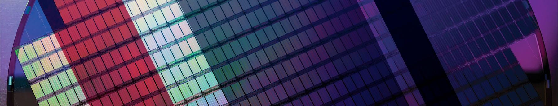
Nanofab: Fabrication
THE NANOFABRICATION LABORATORY
The Materials Research Institute Nanofab provides access to state-of-the-art nanofabrication capabilities and expertise to researchers from academia, industry, and federal research labs. The Nanofab is a 15,000 sq.ft. cleanroom (Class 1000/100) and high-quality support space and is unique in its ability to handle small parts up to 200mm wafers on most tools. The Nanofab staff, in addition to its nanofabrication expertise, has broad experience in condensed-matter physics, chemistry, X-ray physics, optics, and magnetism, offering a broad knowledge base to support the user community. The Nanofab has decades of experience in developing piezoelectric and ferroelectric materials, MEMS devices, heterogeneous integration, and glass packaging. The facility has a long tradition of teaching semiconductor processes to undergraduate and graduate students, and it works closely with industry in developing processes compatible with technology transfer. We are currently working with many semiconductor companies and start-ups that take advantage of our expertise in materials synthesis, integration, and nanofabrication.
MCL: Characterization
MATERIALS CHARACTERIZATION LABORATORY
The MCL is a core facility of the Materials Research Institute and is a fully staffed, open access facility providing access to characterization equipment for materials and devices to enable advanced research while educating the next generation of highly qualified scientists and researchers. The MCL laboratories occupy more than 15,000 square feet within the Millennium Science Complex (MSC) at Penn State and are staffed by interdisciplinary scientists and engineers. Current MCL state of the art capabilities include transmission electron microscopy, scanning electron and ion microscopy, surface characterization, X-ray scattering, molecular spectroscopy, thermal analysis, particle characterization, electrical characterization, and mechanical testing.
AIMI: AI, Machine Learning
CENTER FOR APPLICATIONS OF ARTIFICIAL INTELLIGENCE AND MACHINE LEARNING TO INDUSTRY
Penn State’s Center for Applications of Artificial Intelligence and Machine Learning to Industry (AIMI) connects industry members with Penn State’s vast research community of artificial intelligence (AI) and machine learning (ML) researchers and their students to solve real-world problems and seize market opportunities. AIMI can help your business or organization partner with world experts to explore innovative ways to leveraging AI that addresses your organizational needs, engage directly with faculty and students on short-term, low-risk, high-reward, shared intellectual property development. We develop a comprehensive and diverse workforce pipeline through substantive involvement in shared projects and deliverables.
Digital Twins: Materials Growth & Immersive Interaction
MATERIALS GROWTH SIMULATIONS
Penn State has extensive expertise in simulating materials growth and calculating material properties – covering size ranges all the way from atomistic-scale to the continuum. This involves computational methods including quantum mechanics – in particular: density functional theory, physicsbased and machine learning-based, reactive and non-reactive empirical force fields, phase field- and phase diagram-based methods, and computational fluid dynamics methods. In each of these methods, Penn State provides world-leading method development and application expertise – which established connectivity to experimental efforts in 2DCC and Nanofab.
IMMERSIVE INTERACTION WITH DIGITAL TWINS
By creating a high-fidelity digital twin of physical processes, Penn State can provide a state-of-the-art immersive networking and computing platform to support interactive training, realtime immersive monitoring, and precise control through virtual/mixed reality (VR/MR) headsets. Customizable to suit a diverse range of digital twin applications, we can offer comprehensive guarantees on human performance, ensuring seamless integration and operational excellence from start to finish. These digital twin activities are supported by the Materials Research Institute (MRI), the Institute of Computational and Data Science (ICDS), and the Center for Immersive Experiences (CIE). In support of semiconductor research, ICDS has a number of strategic efforts under its artificial intelligence (AI) Hub. The high performance computing infrastructure maintained by ICDS and its highly qualified staff also enable the handling of large data sets arising from detailed synthesis monitoring, and complex device designs that increasingly need hierarchical spatial and time analytics in their simulations. CIE is driven to catalyze fundamental scientific research efforts through immersive technologies. Using high fidelity and hyper realistic virtual, augmented, and mixed reality experiences, paired with a deep expertise in human factors, advanced simulations, and computer visualizations, our work is easily integrated into research, education, and outreach efforts. Projects in the center range from fully interactive digital twins of complex manufacturing systems to hands-on training to upskill the current and future workforce. Because the scope and potential reach of xR is not limited to any one discipline, CIE’s work is rooted in empirical research and a pedagogical approach to its implementation.
Visit the website to learn more about Penn State research expertise and involvement in the CHIPS and Science Act.